
Can Via Fill Bend and Flex?
Via Fill Bend and Flex
Via fill is an additional process that can be added to the standard PCB manufacturing that increases copper content of via holes. This is used for many reasons including improving etch yield, strengthening pad attachment, solder wicking reduction, silkscreen printing enhancement, and increasing current capacity. It can also help to prevent short-circuits between layers by minimizing the distance between copper traces and pads.
A conductive via fill is made of copper epoxy or silver epoxy that acts as an electrical conductor. It is more expensive than non-conductive via fill, but it offers a number of benefits including improving current flow and thermal conductivity and deviating heat from large components like ICs and BGAs. A conductive via fill is most commonly used for buried or blind vias, but it can also be used for through-hole connections.
The main drawback to a conductive via fill is that the metal will heat up and expand far more rapidly than the surrounding laminate. This unequal expansion can lead to stress fractures between the pad and hole wall. This issue can be mitigated by using a via-in-pad processing technique where the copper pad is plated over the via rather than the hole wall.
However, this is only a viable option when the pad diameter is smaller than the via barrel and it can result in a decreased material strength. The alternative to a conductive via fill is a non-conductive via fill, which can be made of either polymer or epoxy. Non-conductive via fills can be cost-effective and still offer a number of advantages, such as increasing the current density between the pads and eliminating potential short circuits between layers.
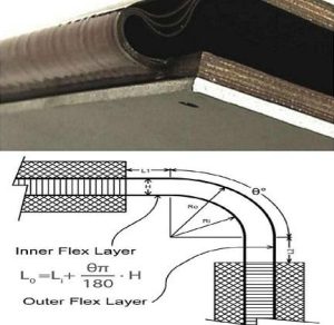
Can Via Fill Bend and Flex?
Non-conductive via fills are also more resilient to bending than through-hole connections. This is because they have a lower coefficient of expansion than the laminate, which distributes stresses more evenly. They can be used for through-hole or blind and buried vias, as well as both through-hole and surface-mount pads.
Vias in flexible printed circuit boards can be subject to significant tensile and compressive stress when the board is bent or flexed, so it’s important to choose an appropriate material for the via fill. A conductive via fill can be more resilient to tensile stress, while a non-conductive via fill can be more susceptible to compression stress.
The most critical thing to remember when choosing a via fill for your project is that it’s important to select an experienced manufacturer. A quality manufacturer will ensure that the vias are properly filled without adding too much copper to the outer layer. Too much copper will increase the weight of the PCB and can cause defects or failure to meet specifications. They will also make sure that the copper is evenly distributed across the pads and traces to avoid stress hotspots.
Utilize controlled impedance routing techniques to match the impedance of signal traces with the impedance of the transmission line. This helps maintain signal integrity and reduces the risk of reflections and signal distortion, which can be caused by signal interference. Use simulation tools and conduct thorough testing to validate the effectiveness of your via fill design. Simulations can help identify potential areas of signal interference and allow you to make necessary adjustments before fabrication.
Leave a Reply